Process Review
TERM PROJECT
Advancement of Transistors through Functional IC Processing
(Brief outline)
By Andrew Cantrell
MSE 442- Brush
Fall
2002
Table of Contents:
Background
Introduction
Integrated Circuits (IC’s) have importance everywhere in our electronic technical age. The demand is for smaller and faster functional electronic devices. An example of a device popular in today’s fast paced lifestyle is cell phones. The major constraint in advancement of cell phone functionally size. Many IC devices are processed using conventional semiconductor technology. So, to increase performance, functionality, and reduce size of electronic devices one must be concerned with electronic packaging and semiconductor fundamentals.
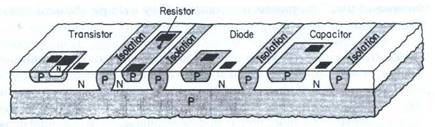
Figure 1: Basic components of integrated circuits. [2]
The following brief discussion of semiconductor technology will focus on only one of the basic components in IC’s, the transistor (figure 1). Classical semiconductor design processes need to be adapted to make the new nano transistors. New functional changes and processing possible for transistor advancements will be discussed. When these functional transistor advancements are applied and commercialized IC technology overall will be advanced. In summary we will outline some semiconductor basics, transistor basics, present advancements, and future improvements.
Semiconductor
Basics
The Czochralski method is the most common process used to grow large single crystal Silicon extrinsic semiconductors. From the large silicon crystals, thin wafers are cut and used as the IC substrate upon which transistors are built. The silicon wafer is then manufactured into a transistor by successive and elaborate steps.
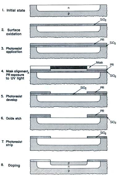
Figure 2: Basic Steps of Photoresist (PR) masking to make p-n-p bipolar transistor. [2]
Doping of the extrinsic semiconductor is the introduction of single elements in the silicon lattice. Doping controls the fundamental characteristics and functionally of the transistor. Doping elements have one additional or one less valence electron than the semiconductor. N-type and p-type doping gives the following different energy band structures (figure 3).
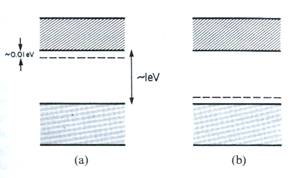
Figure 3: Band Structure a) Donor (n-type) b) Acceptor (p-type) [2]
Transistor
Basics
There are many types of transistors; the major types are Bipolar-junction transistors, Junction field-effect transistors (JFET), and Metal oxide semiconductor field-effect transistors (MOSFET). The major components of transistor are the substrate, source, drain, channel, gate, and gate insulation (figure 4). Generally for FET’s the components are defined: The substrate is a semiconductor (Silicon). Source, Drain, and Channel are all the same type (n-type or p-type) doped region. Channel is the majority carrier path (a low-doped region) from the source to the drain. Gate controls the flow by an induced electric field. The gate insulation protects from leakage and reduced control. [2]
Present
Advancements
Only the benefits of these present advancements for transistors will be discussed given by important transistor characteristics. The four most desired characteristics under research and design for transistors are improve performance, reduce current leakage, increase transistor state control and control of power consumption. The present processing/design solutions for these desired characteristics are 1strained silicon crystalline structure, 2silicon-on-insulator (SOL) wafers, 3gate insulator - dielectric increase, 4metal gates, and 5double gates.
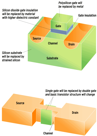
Figure 4: Present Advancements Implied Sketch [1]
1Strained Silicon Crystalline Structure
To improve performance of the transistor the key is to increasing the mobility and/or the effective mass of the majority charge carrier through the channel. This can be done by increasing the lattice spacing (i.e. straining the silicon lattice) in the substrate plane of the transistor. The silicon straining process is as follows:
a) b) c) d)
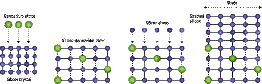
Figure 5: Strained-Silicon Process [1]
a) Add Germanium atoms (same valence as Silicon).
b) Germanium seeded in lattice increasing lattice spacing.
c) Grow pure Silicon layer on top of Germanium seeded lattice.
d) New Silicon layer is strained due to larger lattice spacing below.
2SOL substrate
To reduce current leakage silicon-on-insulator wafers have been used. The object of the buried SiO2 layer is to confine the junction area (i.e. reduce the junction capacitance). Reducing power loss by insulating the boundaries of the junction area, and thus speed up the transistor switching.
3Gate
insulation
The present gate insulation (SiO2) is proposed to be replaced by material with higher dielectric constant to reduce current leakage.
4Metal
gates
Metal gates are proposed to control power consumption, due to their large amounts of charge carriers (sea of electrons).
5Double
gates
The double gating fin field effect transistor (finFET) system has been researched and shows a promising future. These finFET’s may well replace the classical one gate and boost performance while reducing leakage. These transistors could be useful in a thermal management aspect as well.
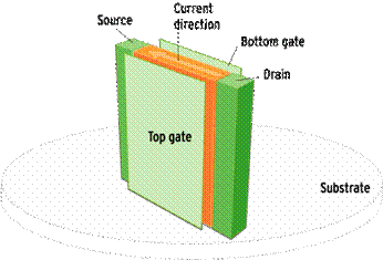
Figure 6: finFET sketch [1]
Conclusion
All the presented research and design solutions in
transistor processing still have many thermal, chemical, and mechanical
compatibilities problems before they are complete working solutions in the
commercial market. Out of all of the proposed advancements discussed the
strained Silicon crystalline lattice is the best working solution (as stated by
IBM [2]) In conclusion, we can
clearly state that as the world moves to a more electronic future the
performance of transistors can only increase, and the size only decrease. Thus
the IC processing will become an even more important factor in electronic
device building. Also the need for more electronic efficiency should drive the
present planar transistors out of classical semiconductor device technology and
into something new. We can also say future advances in electronic devices will
rest upon the development and understanding of material properties; and
electronic packaging requirements for any future applications of transistors.
Reference(s)
1)
The Amazing Vanishing Transistor Act by Linda Geppert
IEEE October 2002
2) Electronic Properties of Materials (Third Edition) by Rolf E. Hummel
Copyright 2001,1993,1985 Springer-Verlag New York, Inc.
3)
Electronic Packaging: Design, Materials, Process, and Reliability
by John H Lau, C.P. Wong, John L. Prince, and Wataru
Nakayama
Copyright 1998 McGraw-Hill
4) Quick Study Charts: Electronics I & II
Copyright 2002 BarCharts, Inc.
5) Thanks to: Professor Lucien N. Brush
Helped in review and editing of the rough draft.