Self-Assembly & Nanomaterials
Nanostructured materials represent a fascinating class of materials whose structural elements such as atomic clusters, crystallites or molecules have dimensions in the range of 1 to 100 nm, the length scale that defines physical properties of materials and at which intriguing phenomena are observed due to quantum phenomena. They exhibit unique electrical, optical, magnetic, mechanical and sensing properties that are readily tunable through controlling their size, and enable novel applications that are impossible to realize with their bulk counterparts. Zero-, one- and two-dimensional nanostructured materials such as metallic or semiconducting nanoparticles, quantum dots, carbon nanotubes, nanowires, graphene, 2-D nanosheets, supramolecular nanostructures and polymeric dendrimers, and nanopatterning techniques such as e-beam and nanoimprinting lithography have been well established or are being actively developed. One key step towards novel applications of nanostructured materials concerns their surface functionalization, assembly, patterning, orientation and alignment into functional networks with enhanced or unprecedented properties. Among the bottom-up strategies, self-assembly provides a promising route to build up complex systems with immense flexibility in terms of nanoscale building blocks and resulting functionalities and properties. As the name suggests, self-assembly is a process in which organization of colloidal, macromolecular, or supramolecular units into the desired system occurs through nature-intended phenomena, either mediated by physicochemical pathways or assisted by biomolecules to promote molecular selectivity and specificity. Our strategy is to combine molecular/biomacromolecular self-assembly with nanostructured materials for electronic, photonic and biological applications. Current research is mainly focused on (1) fundamental understanding of molecular self-assembly on surfaces, (2) multifunctional self-assembled molecular materials for field-effect transistors, (3) nanopatterned molecular interface and self-assembled electron-acceptors for high-performance solar cells, and (4) bio-enabled and patterned nanosystems for plasmonics and bionanotechnology.
Fundamental Understanding of Molecular Self-Assembly on Surfaces
Novel aryl thiol and p-sigama-phosphonic acid molecules are rationally designed, synthesized, self-assembled or patterned on surfaces of metal (Au, Ag), semiconductor (Si, GaAs), metal oxide (ITO, SiO2/Si, AlOx, HfOx, TiOx, ZnO), or nanomaterials (NP, QD, nanowire, graphene, 2-D nanosheet). Diversified molecule-molecule and molecule-substrate interactions are utilized to form dense and well-packed self-assembled monolayers (SAMs) and tailor novel nanoelectronic/optical behaviors, surface reactions and interfacial properties for optoelectronic devices. The quality of molecular SAMs is investigated through AFM (smoothness and uniformity), contact angle (surface energy), ellipsometry (thickness), FTIR (order, binding mode and functional groups), XPS (surface component), SFG and NEXAFS (tilt angle, orientation of terminal group). Photon-STM and SERS are used to monitor molecular motions and reactions under nano-environment and understand/measure complex chemical reaction, ground state, excited state, light absorption, charge separation, charge generation and charge transport of molecules on surfaces.
Multifunctional Self-Assembled Molecular Materials for Field-Effect Transistors
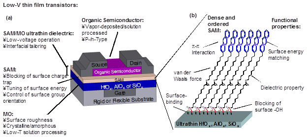
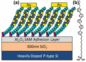
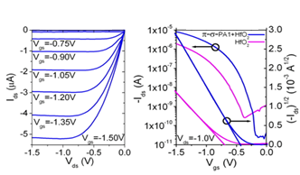
p-sigama-Phosphonic acid SAMs on nanolayers of metal oxides, such as hafnium oxide and aluminum oxide, are shown to enable (a) low-voltage (sub 2V) organic field-effect transistors (OFETs) through dielectric and interface engineering on rigid and plastic substrates, (b) simultaneous one-component modification of source/drain and dielectric surfaces in bottom-contact OFETs, and (c) SAM-FETs based on molecular monolayer semiconductors. Novel multifunctional self-assembled molecular materials are being designed and synthesized for high-performance, low-voltage thin-film transistors (TFTs), monolayer-based FETs, photo-transistors and graphene devices to realize low-power, low-cost flexible electronics and optoelectronic circuits.
Nanopatterned Molecular Interface and Self-Assembled Electron-Acceptors for High-Performance Solar Cells
There is an urgent need for alternative acceptor materials that – like PCBMs – possess favorable electron-transporting and processing properties, but which also absorb strongly in the solar spectrum, have energy levels significantly different from those of fullerene-based acceptors, and exhibit diversification regarding derivatization and functionalization. In addition, it is desirable to have electron acceptors with the combination of tunable molecular structures, controlled nanomorphology in electron donor (D)/acceptor (A) blends, and tailored D/A interfaces in optimized device architectures, which allow maximized exciton generation/migration and charge separation/transport/collection. Our approaches are to design and synthesize electron acceptors through tailoring of p-conjugated core/bridge and peripheral group to have tunable energetics (bandgap, HOMO, LUMO), and introducing thermo-/photo-removable, hydrogen-bonding and surface-binding groups to allow processability, monolayer-templated self-assembly and nanophase formation for optimized charge transport and collection, and fabricate/test inverted polymer solar cells by utilizing patterned monolayer-induced assembly of D/A nanophases toward high power-conversion efficiency and good stability.
Bio-Enabled and Patterned Nanosystems for Plasmonics and Bionanotechnology
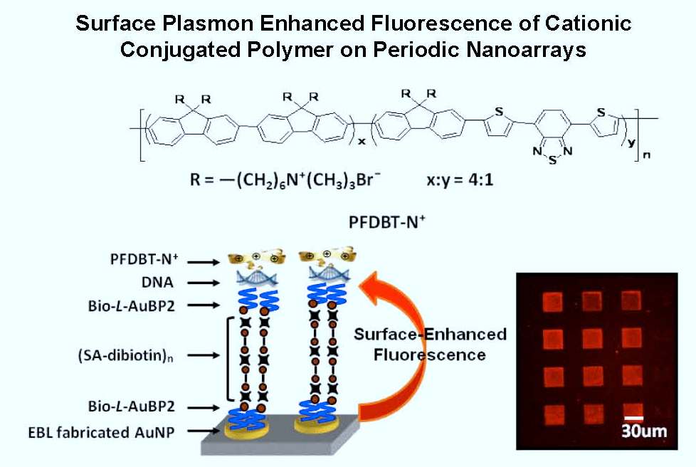
Inorganic nanostructures exhibit unique electronic, optical, and catalytic properties that can be used in nanoscale assemblies to alter the photophysical properties of nearby emitters. Meanwhile, p-conjugated polymers/organic semiconductors possess electrical, optical, and opto-electronic properties which can be tailored by rational molecular design and have the ability to amplify a chemical signal into a measured electrical or optical event. In addition, genetically engineering polypeptides for inorganic surfaces can be tailored to have surface selectivity, molecular recognition, and functionality. Hence, our efforts have been devoted in studying hybrid nanosystems with these combined building blocks for potential applications in nanophotonics, electronics and bionanotechnology. Surface plasmon enhanced tunable p-conjugated polymer or QD nanoarrays have been demonstrated where a 16-fold or 15-fold increase in the p-conjugated polymer or QD photoluminescence is observed.
In the Media
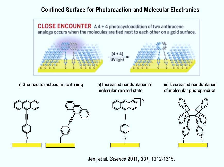
Kim, M., Hohman, J. N., Cao, Y., Houk, K. N., Ma, H., Jen, A. K.-Y., Weiss, P. S., “Creating Favorable Geometries for Directing Organic Photoreactions in Alkanethiolate Monolayers”, Science 2011, 331, 1312. (Highlighted on Chem. & Eng. News, March 14, 2011. Highlighted by UW Today, March 15, 2011. Highlighted by UCLA Newsroom, March 10, 2011.)
http://pubs.acs.org/cen/news/89/i11/8911notw7.html
Chemical & Engineering News MARCH 14, 2011 VOLUME 89, NUMBER 11 P. 12
Poised To React
Nanoscience: Tethering molecules to gold surface forces reaction
Bethany Halford
“Controlling a single molecule’s reaction with light could improve solar cells”
UW Today |March 15, 2011
http://www.washington.edu/news/articles/controlling-a-single-molecule2019s-reaction-with-light-could-improve-solar-cells
By Hannah Hickey
News and Information
“New method for studying molecule reactions a breakthrough in organic chemistry”
UCLA nanotech research mimics enzymes in directing chemical reactions
By Mike Rodewald March 10, 2011
UCLA News Office | March 10, 2011
http://newsroom.ucla.edu/portal/ucla/nanotechnology-method-for-studying-193118.aspx