
Scanning Probe Microscopy
Many emerging materials—such as new semiconductors for converting sunlight into electricity, and mixed conductors for use in bioelectronics and batteries—are structurally complex. Their performance depends on both local chemical composition as well as morphology and ordering at length scales of a few nanometers to hundred nanometers.
We use scanning probe microscopy to probe the properties of such materials at nanometer length scales well below the diffraction limit. We combine optical excitation with electrical and mechanical detection using a scanning probe tip to connect local structure with the performance of semiconductor optoelectronic device performance. The goal of the AFM research in our lab is to make the study of dynamic behaviors in condensed phase, nanostructured materials just as routine as the use of conventional, diffraction-limited, optical microscopy. We do so in the context of important challenges, such as understanding the performance of emerging energy materials such as hybrid organic-inorganic perovskites.
We make extensive use of Atomic Force Microscopy (AFM) methods. AFM uses a sharp metal tip affixed to a micro-fabricated cantilever beam akin to a diving board. By bringing this tip in close proximity to the surface we can interrogate local information.
Typically, the tip is oscillating at a given frequency depending on the resonance behavior of the beam, and this resonance frequency will shift depending on the local electrostatic forces (among other things).
In a more basic mode of operation, the tip can instead drag along the surface in a manner (contact mode) and then measure the current through the tip much like a device measurement at each pixel.
We have pioneered the application of a wide range of AFM techniques over the years that each probe different physical parameters.
These include:
- Photoconductive AFM (pcAFM) – measures the photocurrent at each pixel in a photovoltaic device
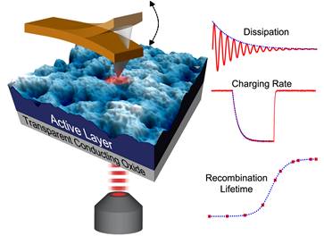
- Time-resolved electrostatic force microscopy (trEFM) – measures the local charging rate due to build up of charges due to voltage and/or photoexcitation; in solar cells this is correlated with device-level external quantum efficiency
- Intensity-modulated scanning Kelvin probe microscopy (IM-SKPM) – measure the local carrier recombination lifetime based on the decay of surface photovoltage; this method can be quantitatively similar to device-level transient photovoltage measurements
- Cantilever ringdown – uses the decay of the cantilever amplitude due to changes in the local energy dissipation to quantitatively map out changes in the quality factor Q; this technique is useful for looking at trapping in films, for example
- Fast-free trEFM (FF-trEFM) – uses the physics of cantilever motion to extract sub-microsecond changes in the resonance frequency
We have primarily developed these in the context of photovoltaics but they are applied to a wide range of materials in our lab, including ionic transport materials for battery and bioelectronics applications, for instance.
For further information, please consult a few of our review articles on the subject: