-
Facilities
Courses
RESEARCHMission Statement
Overall research goal of NanoManufacturing Lab is 'nanoengineering for low cost, rapid diagnosis of diseases'. The major goals are (1) to discover fundamental science of molecular manipulation and detection, in particular, using an electric field, (2) to develop high throughput nanomanufacturing methods, and (3) to apply the fundamental science to a biomedical problem, 'low cost, rapid diagnosis of diseases'. Nanotip enrichment and detection systems
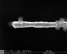
The enrichment and detection of rare molecules are crucial for disease diagnosis, drug delivery and discovery, and environmental monitoring. However, current methods are very limited due to extremely small mass and dimension. Using a nanostructured tip, molecules are enriched and detected with high efficiency. The fundamental science on a nanotip is being explored with development of nanostructured tools. The figure shows polystyrene nanospheres captured on a nanotip. Biomimetic Cilia Bio-Reactors
A challenge of microscale mixing is in relatively low inertia and large viscosity. To overcome this challenge, a highly compliant cilia made of polydimethylsiloxane has been fabricated and resonated in microfluidics. The novelty of this research is in the manufacturing to fabricate a highly compliant structure in solution. The construction of such low-stiffness structure is challenging due to dominant surface tension and high interfacial energy. To overcome this issue, the underwater fabrication method has been developed to construct the cilia in solution. Through this method, an array of cilia has been successfully fabricated for a bioassay. Currently, a further enhanced manufacturing method is being devised and tested for high throughput bioassays. The complex fluid flow generated by the cilia could enhance bioreaction by two orders of magnitude, which will impact drug discovery and genetic expression through bioreactors compatible with microtiter plates. 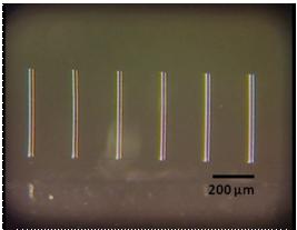
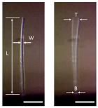
Silicone cilia, resonating cilia, and cilia microwell plates compatible with 384 microplates. Nanofabrication
A major challenge of nanostructured biosensing platform is high throughput, low cost manufacturing of nanostructures. A novel approach using the shadow effect in high vaccum evaporation has been developed for nanostructures including nanochannels, nanowires, and nanojunctions. Unlike the previous nanofabrication methods using the shadow effect, this shadow edge lithography method compensates the evaporation angle variation through the thickness compensation of the shadow mask. This compensation enables the tolerance of 2 nm in a whole Si wafer. This fabrication method is being used for wafer-scale fabrication of nanostructures, which will be used for biomedical applications. 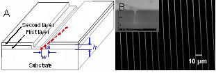
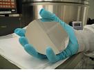
Working principles of Shadow edge lithography, nanochannels, and nanostructures on a 100 mm wafer