Facilities
We have dedicated laboratories for thin film deposition, synthesis and processing of colloidal nanocrystals including their self-assembly, magnetic and transport measurements and materials characterization with electrons, photons and scanning probes.
The Physical Properties Measurement Laboratory (Wilcox 134 and Roberts 221), funded partially through the M. J. Murdock Charitable Trust, that contains:
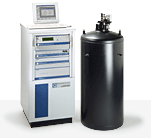
- Quantum Design Physical Properties Measurement System with options to measure heat capacity, magnetometry, electro-transport and thermal transport
- NETZSCH LFA 427 laser flash annealing system capable of high precision heat transport measurements
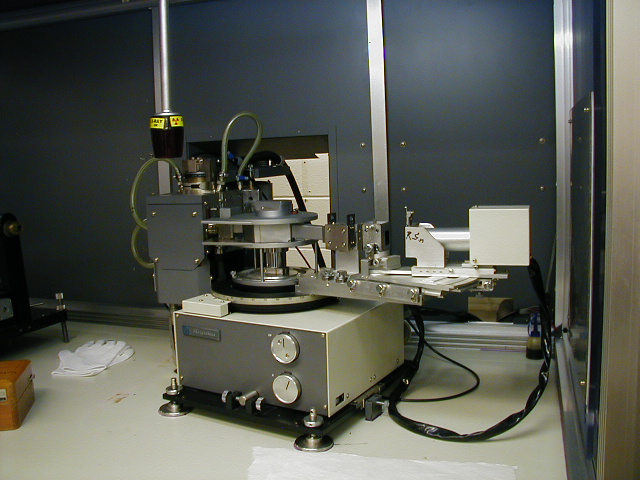
- West Bond Ultrasonic bonding system for device construction
- Probe station for device testing and diagnostics
- Agilent Technologies Spectrum analyzer and a Keithley 6340 sub- femtoamp sourcemeter
- Lakeshore vibrating-sample magnetometer with a 1.8 T electromagnet and sensitivity of 10^-5 emu. The VSM includes a furnace capable of heating samples to 800_C. In addition, there is also a home-built variable temperature (80 K < T < 300 K) resistivity probe, a variable range current source and a high sensitivity multimeter for magneto-transport measurements
- A magneto-optic Kerr effect measurement system, with a .5T magnet, PEM, lock-in amplifier, bipolar power supply, and laser optics for magnetic surface measurements
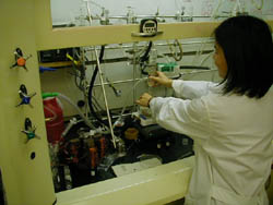
The Chemical Synthesis Laboratory (Wilcox 130) is fully equipped for making and characterizing nanocrystals starting from air-sensitive precursors. This includes:
- An environment-controlled glove box with an in-built refrigerator
- Malvern Dynamic Light Scattering system
- Five Schlenk lines
- Two large fume hood
- Centrifuges
- Ultra-sensitive balance
- Ovens
- Refrigerator
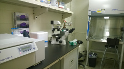
In our BSL-2 certified Cell and Tissue Culture Laboratory, we investigate the in vitro and ex vivo performance of the nanoparticles produced in our chemical synthesis laboratory. We are also authorized to do our nanoparticles pharmacokinetics and biodistribution studies in University of Washington animal facilities. We actively collaborate with other laboratories and research centers across the campus for doing confocal microscopy, animal imaging using MRI and IVIS and doing the tissue harvesting, histology and confocal microscopy.
This BSL-2 certified laboratory contains:
- Bio-safety cabinet
- Centrifuge
- Optical microscope
- Incubator
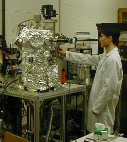
The Thin Film Laboratory (Wilcox 132) houses:
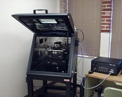
- A computer-controlled UHV ion-beam deposition system that is used to prepare high quality thin film heterostructures. It is equipped with a Kauffman-type source (2.5 cm), four independent targets, a heater block capable of achieving substrate temperatures of 1000 _C, an oscillating crystal thickness monitor, a residual gas analyzer for process monitoring, mass-flow controllers capable of independently handling three different gases for reactive sputtering, and a linear feed-through shutter with motorized control for making wedge-shaped samples. The library of targets for sputtering includes a wide range of magnetic/noble metals and alloys.
- A magnetron sputtering system, featuring RF and DC power supplies, three 1" sources and substrate heating to 1000_C is also available. The system is dedicated largely for the synthesis of thin oxide films.
- A vacuum evaporator
- A spin-coater for sol-gel synthesis of thin films, and two furnaces (box and tube, rated to 1100_C) for annealing under controlled environments.
The Structural Characterization & Imaging Laboratory contains:
- A 12 kW Rigaku rotating anode x-ray generator with a powder theta - 2theta diffractometer and a second double crystal diffractometer for thin film analysis.
- For Surface Characterization, an atomic force microscope purchased from Asylum Research, Inc., has been installed. This particular model can perform not only atomic force microscopy (AFM) and magnetic force microscopy scans, but also conductive AFM measurements with a sensitivity ranging from hundreds of femtoamps to one microamp are also possible. Imaging has a maximum resolution of 25 megapixels.
- In addition, we have acquired and installed a Philips 420 TEM/STEM with EDXS capabilities for routine electron microscopy, diffraction and microanalysis.