The 'Optical Density Board' or 'OD Board' powers the red wavelength laser which is used to determine the turbidity of a given culture. One OD Board is attached to each 3D printed culture tube holder, so for an array of 8 turbidostats you will need 8 OD boards. The OD Board houses two photo-detectors that measure the quantity of light sent from the source and that which is transmitted through the culture. In this way an increase in culture turbidity will result in a decrease in signal in the second sensor. The quantity of light transmitted through the culture, normalized to the quantity of light sent from the source are communicated to the 'Main Controller Board' or 'Main Board' via an either-net cable and used to control the pump dilution rate to maintain a desired optical density.
Ordering the assembled PCBs
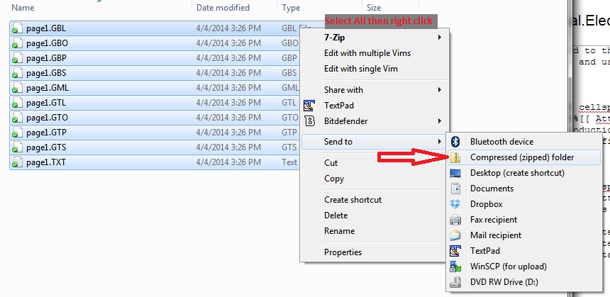
| Step 1. Zip the production files.
- from the root of the design files find the directory led_board/PCB/production_files and zip it's contents.
|
|---|
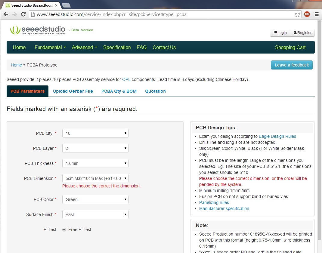
| Step 2. PCB Parameters
|
|---|
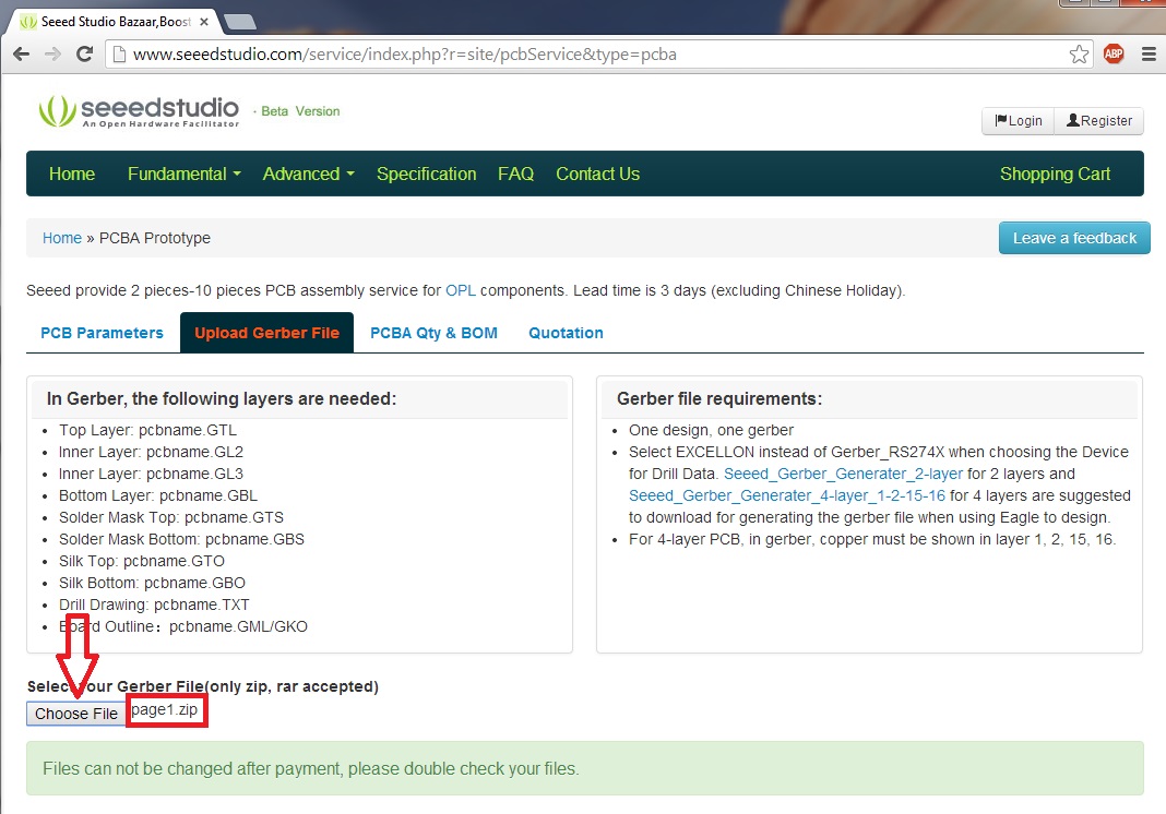
| Step 3. Upload Gerber File
- Press the "Choose File" button and select the zip file you just made in step 1.
- Click next.
|
|---|
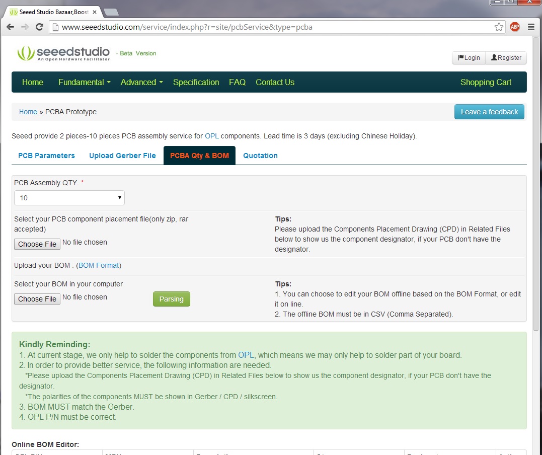
| Step 3. PCBA Qty & BOM
- Select quantity 10
- Do Not upload any placement file
- Choose the file led_board/PCB/seeed_BOM_File.csv as the BOM file
- press the button labeled "Parsing"
- A list of parts under the "Online BOM Editor" heading should appear.
- Click next.
|
|---|
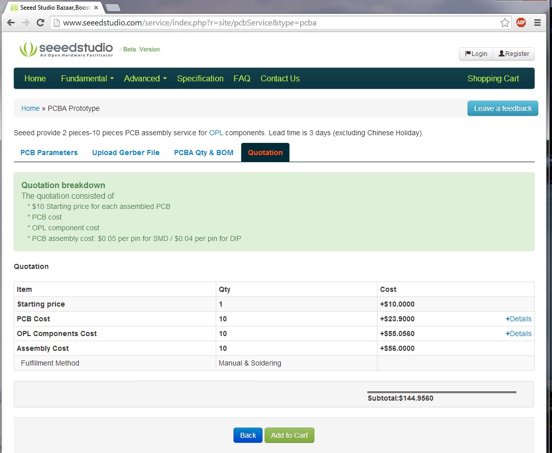
| Step 4. Quotation
- Check that everything looks right. At the time of this writing the quotation came out to $144.9560. Prices on electronic components vary as a commodity, as do labor costs so your quotation may differ slightly in price.
- Choose "Add to Cart" and check out
- Note: We strongly recommend not choosing the default shipping method as it can take upwards of 30 days.
|
|---|
Finishing Touches
There is one component, the light sensor, that Seeed Studio cannot solder for us. I recommend using leaded solder as it is easier and joints are more robust. Note that the following steps should be repeated for each OD board.
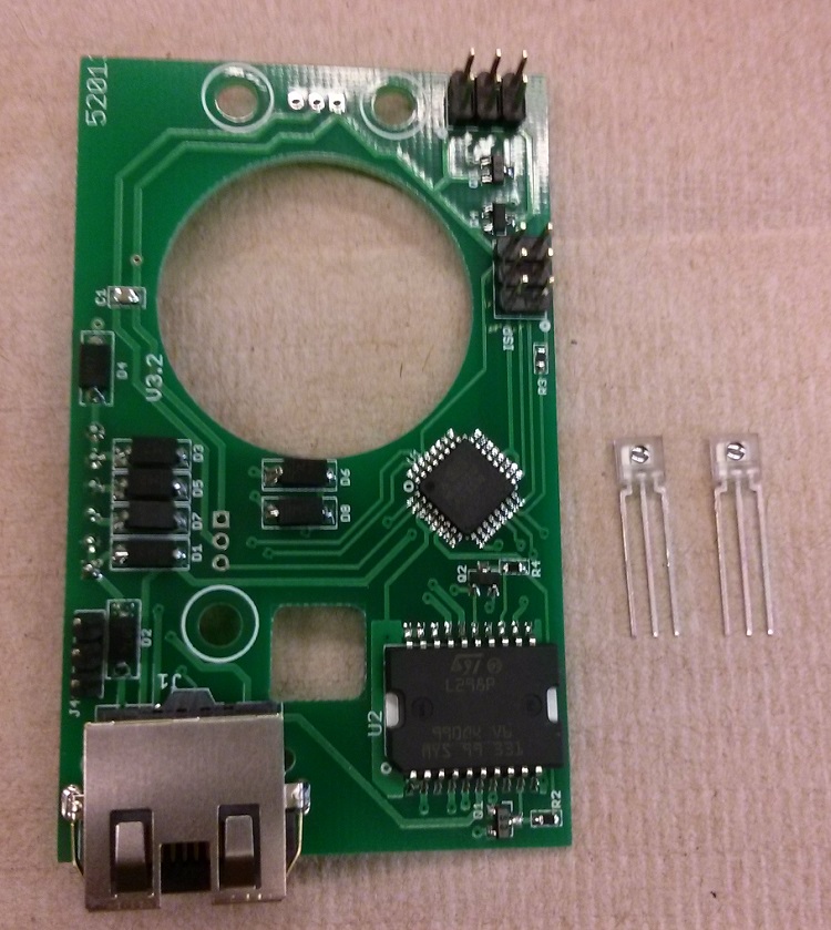
| Step 1. Collect a circuit board and two light sensors.
|
|---|
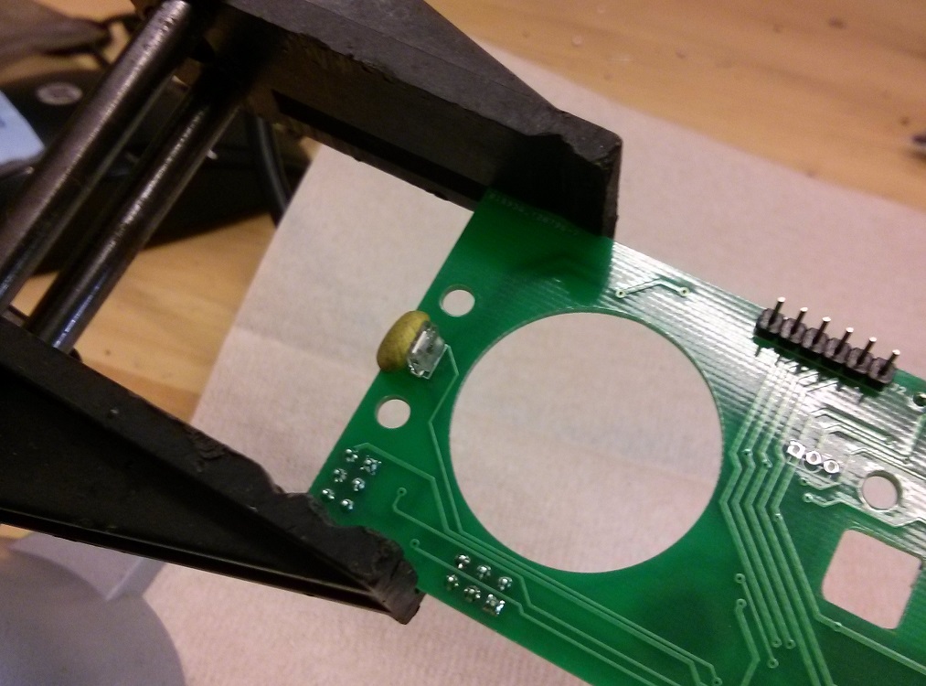
| Step 2. Solder the first light sensor in place
- Insert the first light sensor so the dome faces the center of the PCB. Make sure that you insert the light sensor on the back side of the circuit board (see photo).
- a small ammount of tape or poster tack will help hold the part in place as you solder
- Turn the board over and solder the component into place.
|
|---|
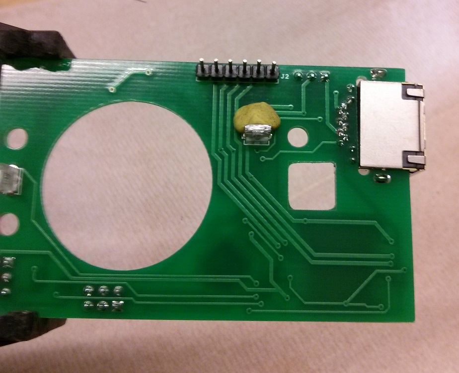
| Step 3. Solder the first light sensor in place
- Repeat for the second light sensor. Again, this sensor should be on the back side of the PCB and face inward.
|
|---|
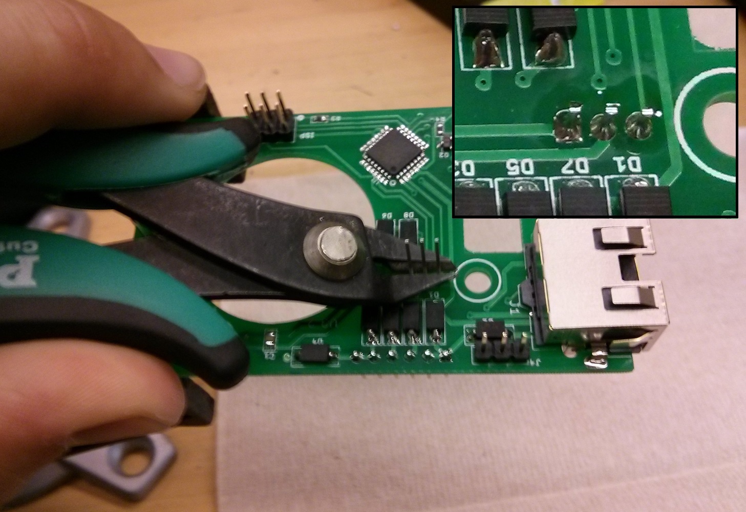
| Step 4. Trim the leads
- Trim the light sensor leads to just above the solder join. This prevents accidental shorting.
|
|---|
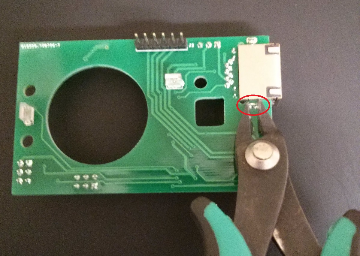
| Step 5. Trim inside tab off of the ethernet jack.
- Trim the inside tab off of the ethernet jack. This prevents mechanical interference between the laser and the circuit board. Try and trim the solder tab as close to the PCB as possible. Don't worry about damaging the PCB as there are no traces near by and the tab you are cutting has no electrical function.
|
|---|


